PCB fabrication facility created in the School of Engineering, Mathematics, and Physics (EMP)
By: Communications

UEA's School of Engineering, Mathematics, and Physics (EMP) has put into place a PCB production facility for the fabrication of Printed Circuit Boards (PCBs) and construction of prototype electronic circuits using through hole and surface mount components, thanks to concerted effort from EMP students Jack Bobbin and Robert Avery with technical support from David Ciplic (ENV) and Nick Griffin (ENV) and overall supervision from Dr Dennis Fitzpatrick (EMP).
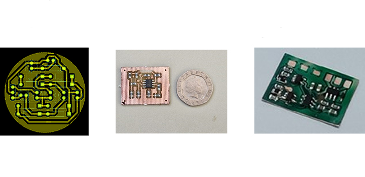
The process starts with PCB layouts that are designed using the industry-leading Cadence-OrCAD PCB Editor software. The software outputs standard Gerber files to drive an LPKF PCB milling machine to mill out the pattern of copper tracks on a PCB (Fig.2a). There are three types of PCBs that can be fabricated:
1) Through hole, where components are normally placed on the top side of the board and their connecting leads pushed through and soldered on the bottom side (image below, bottom left)
2) Surface mount, where components are directly soldered onto copper pads (image below, middle)
3) Flex circuits, where components are soldered onto a thin flexible substrate instead of a solid PCB. The flex board weighs less than 0.3g (image below, right)
As part of the surface mount process, the LPKF milling machine also dispenses solder paste onto the copper pads of the milled PCB. An automatic Pick and Place machine is then used to accurately place the surface mount components onto the PCB that is then placed in a solder reflow oven where the solder paste melts and effectively solders the components to the board. Surface mount boards are now considered the industry standard for electronic circuits not only for their small size but also for the significant reduction in component costs compared to through hole components.
The PCB production unit will enhance Engineering student's experience of using the latest techniques and processes used in industry for electronic circuit design and production. There is also the cost and time saving associated with student PCBs being made at UEA rather than the usual one to two weeks turnaround from external companies.
The PCB facility will also be available to external companies that require the manufacture of PCBs for prototype electronic circuits.
Please contact Dr Dennis Fitzpatrick for more information.
Related Articles
UEA scientist leads Westminster call for sustained investment in astrophysics
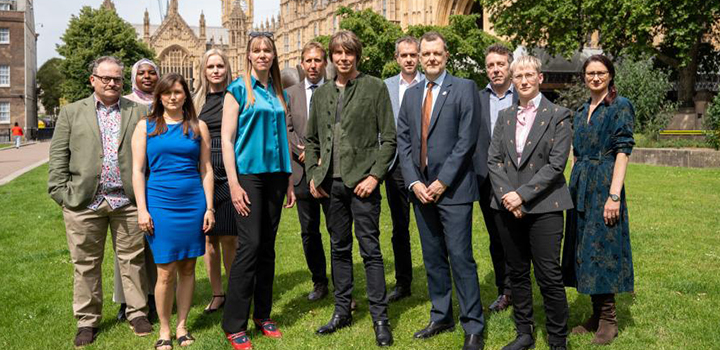
A space scientist from the University of East Anglia (UEA) joined forces with TV’s Brian Cox and MP Clive Lewis to campaign for continued investment in astrophysics at Westminster yesterday.
Read more
UEA’s grant and funding success – January 2026
Discover the latest research and funding grant successes happening within the University of East Anglia.
Read more
UEA and Hethel Innovation building on solid foundations with new Memorandum of Understanding
UEA and Hethel Innovation have strengthened their longstanding collaborative partnership with the formal signing of a strategic Memorandum of Understanding, recognising a shared commitment to innovation and sustainable economic growth.
Read more